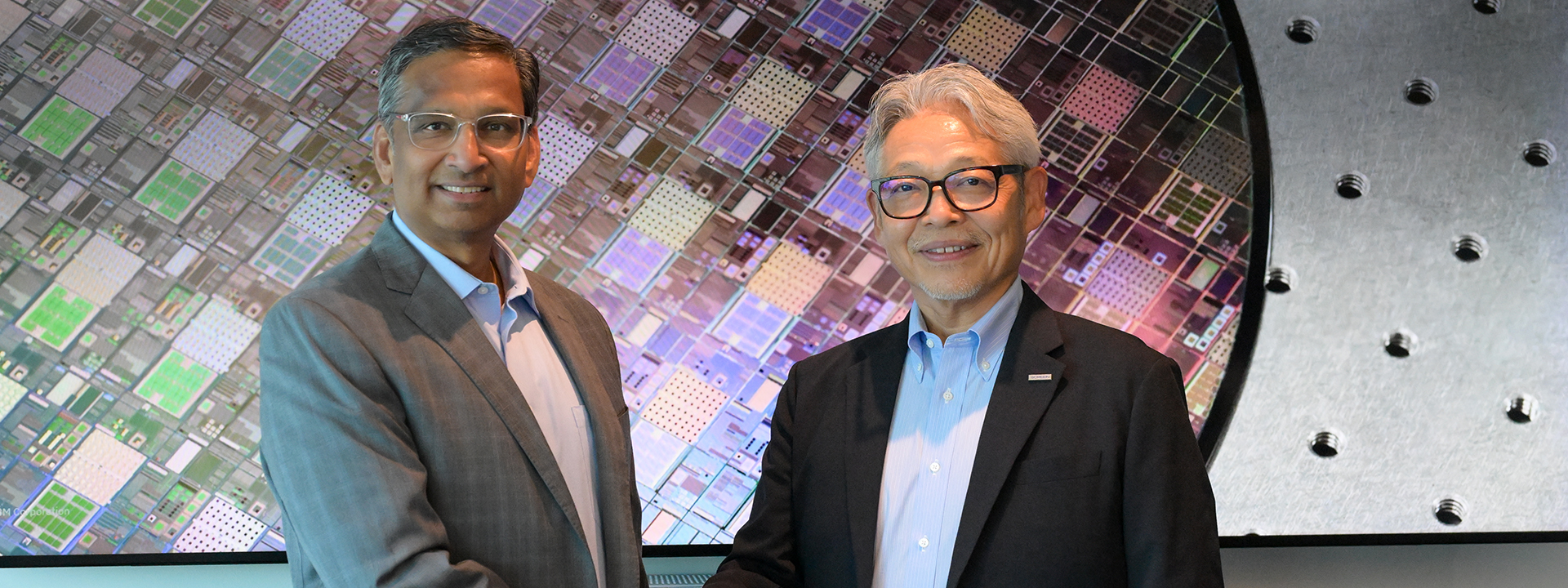
Albany, NY / Kyoto, Japan – September 24, 2025 – IBM and SCREEN Semiconductor Solutions Co., Ltd. have entered into a new agreement to develop cutting-edge cleaning processes designed for High Numerical Aperture (High NA) EUV lithography. The partnership builds on more than a decade of collaboration between the two companies in semiconductor process innovation.
Why This Matters
With the global demand for smaller, faster, and more efficient chips driving semiconductor manufacturing, advanced lithography is becoming essential. High NA EUV, often regarded as the next frontier beyond the 2nm process node, presents new challenges in wafer production. Even the tiniest particles or surface defects can significantly impact performance, making wafer cleaning a critical step in ensuring yield and reliability.
Combining Strengths
- IBM brings expertise in semiconductor process integration and full-stack development, supporting innovation for AI-era computing.
- SCREEN contributes its global leadership in wafer cleaning technologies, where it holds the top market share in semiconductor cleaning equipment.
Together, the companies will develop next-generation cleaning techniques capable of meeting the stringent demands of High NA EUV, ensuring robust and scalable solutions for device manufacturers.
Industry Impact
This collaboration aims to accelerate the transition to sub-2nm manufacturing and support the development of smaller, more powerful chips that will power advancements in AI, hybrid cloud, and other emerging technologies. By addressing one of the most complex bottlenecks in the chipmaking process—cleanliness—IBM and SCREEN are paving the way for reliable next-generation semiconductor production.
Leadership Voices
- Mukesh Khare, GM of IBM Semiconductors, highlighted High NA EUV as “critical for enabling smaller, more powerful semiconductors in the age of AI.”
- Akihiko Okamoto, President of SCREEN Semiconductor Solutions, emphasized the value of combining SCREEN’s precision cleaning expertise with IBM’s process development flow to meet the requirements of advanced chipmaking.
Disclaimer
This article is prepared for informational and educational purposes only. It is based on publicly available press releases and announcements from IBM and SCREEN Semiconductor Solutions Co., Ltd. The content is an original rewrite and is not an official statement from either company. For the official press release, please visit IBM’s newsroom or SCREEN’s corporate website.